(China (Mainland))

Product Summary
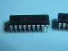
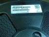
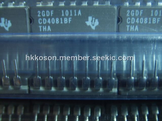
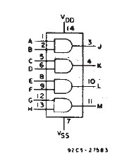
The CD4081BF is a CMOS AND gate which provides the system designer with direct implementation of the AND function and supplement the existing family of CMOS gates. The CD4081BF is supplied in 14-lead hermetic dual-in-line ceramic packages.
Parametrics
CD4081BF absolute maximum ratings: (1)DC supply-voltage range, VDD: -0.5 to +20 V; (2)input voltage range, all inputs: -0.5 V to VDD+0.5 V; (3)DC input current, any one input: ± 10 mA; (4)power dissipation per package: 500 mW; (5)device dissipation per output transistor for TA=fullpackage-temperature range: 100 mW; (6)operating temperature range: -55 to +125℃; (7)storage temperature range: -65 to +150℃; (8)lead temperature: +265℃.
Features
CD4081BF features: (1)medium speed operation: tpHL, tpHL=60 ns at VDD=10 V; (2)100% tested for quiescent current at 20 V; (3)maximum input current of 1 μA at 18 V over full package-temperature range: 100nA at 18V and 25 ℃; (4)standardized symmetrical output characteristics; (5)5-V, 10-V and 15-V parametric ratings.
Diagrams
 |
 CD4000B |
Other |
|
Data Sheet |
Negotiable |
|
||||
|
CD4000BMS |
Other |
|
Data Sheet |
Negotiable |
|
||||
|
CD4001BC |
Other |
|
Data Sheet |
Negotiable |
|
||||
 |
CD4001BCM |
|
IC GATE NOR BUFF QUAD 2IN 14SOIC |
Data Sheet |
Negotiable |
|
||||
|
CD4001BCMX |
|
IC GATE NOR QUAD 2INPUT 14-SOIC |
Data Sheet |
Negotiable |
|
||||
 |
CD4001BCN |
|
IC GATE NOR BUFF QUAD 2IN 14-DIP |
Data Sheet |
Negotiable |
|
||||